Running DeepSeek-R1 on refubrished blade server: 02 Power
Welcome back, Previous part here: Running DeepSeek-R1 on refubrished blade server: 01 Introduction.
Introduction/Plan
I am trying to build server for running DeepSeek-R1 on used supermicro blade, this part will cover my extermination with powering it on.
Reverse engineering server hardware and messing with power supplies can be risky. Please, be extremely careful in doing so. I am not responsible if something blows up.
Again let's start with basic plan:
- Figure out how to connect 12V to it.
- Figure out how much power do we need
- Implement
- If fails debug, try implementing it another way
Connecting
Let's start with dissecting original case:
 Link to case manual
Link to backplane manual
Looks like not whole a lot of components here, and very little logic. I decided to assume that Supermicro engineers are lazy (like I am) or they trust there is no dumbass (like me) who would try to power it directly from 12v. Simple short circuit check with multi-meter reveals: Side of connector that faces board is 12V, and the other one is GND.
Power requirements
Let's serach for original power supply. Little googling after, I found that it's 2x12v 2000w redundant PSUs.
This power supplies are for 4 nodes each (500w per node), but since they are Enterprise grade, there is non zero chance that they can push a little bit more over spec.
To be sure, I decided to get approx max power consumption just based on components:
- 2xCPU, 65w each
- 16xDimms, up to 10w each, 160w
- Motherboard, 50-100w To give room for CPU upgrades, I assumed that up to 150w per cpu is possible. This lands us on 500-550w, confirming previous assumption based on original PSU.
Requirements:
- I will need 12v only
- ATX is too thick
- Server PSUs could be harder to connect
Based on those I decided to choose: Mean Well LRS-600N2-12 It's:
- 12v
- 600w
- N2 Series of LRS can deliver bursts of even more (if needed)
- Fits in 1u
- Mostly quite
- Un-standard form factor, but fits in 1U space
- Cheap
- Mean Well is mostly good manufacturer of industrial PSUs.
Implementation, Type-0
Plan:
- Solder contacts directly to connector, as temporary solution (this is temporary solution while debugging, never solder power wires to flat pads.)
- Connect it to power supply
- Try to power it on, connect PSU with power meter in between to better understand what happens.
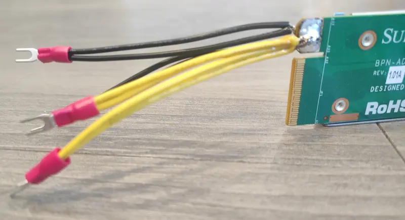
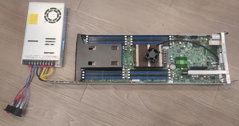
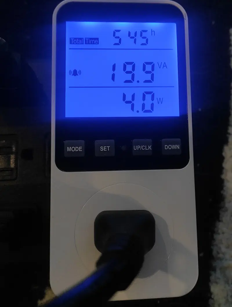 Aaaandd... nothing happens, PSU consumes 4W, fans doesn't start, IPMI1 Ethernet doesn't seem to connect.
I've also tried connecting to vga port; checked voltages on fanheader, USB, Sata power connector all of them show 0. That’s when I realized something critical was missing.
I guess Supermicro engineers aren't as lazy as I expected.
Reverse engineering backplane adapter
Two most important take from the chapter to the reader:
- RTFM, sometimes manufacturer will include pinout (In my case, I didn't found one)
- "reverse engineering if anything is more like playing Sudoku, your main goal isn't to find and answer, but try to reduce field of possibilities."
Basically there is several technics that best work in conjunction:
- continuity checks
- voltage checks
- checking pins with logic analyzer
- making a copy of PCB
I decided that easiest way for me would be to try and make a copy of PCB and check voltages and continuities. Starting with making copy of PCB there is also three ways of doing it:
- Using high resolution X-ray (best and professional way, allows to do multilayered PCBs easily)
- Desolder every component, scanning on flatbed scanner.
- Take photo, and hope that it would be perfectly straight (most non destructive, and cheap)
- Use zoom lens if you have one, it will reduce wrapping, I used Samsung DSLR from 2013 with 20-50mm lens, just because lens correction would be easier then on smartphone.
- Use tripod
- Use as much light as possible (be careful with flash as it can introduce unwanted glare, if you have ring one, it should work)
- Close aperture as tight as possible, f/16-f/22 for maximum sharpness.
- Don't try to take whole board as one photo, sticking one to another is much easier than not seeing traces at all.
Here short guide how to do 3rd option:
- Take photos
- Using darktable or any other software, apply lens correction (and hopefully your lens is in database)
- Export
- Use hugin to semi-automatically stitch your photos
- Use rectilinear projection (straight lines would be straight-ish, but check maybe something else would yield better results in your situation) BUT USE SAME PROJECTION FOR BOTH SIDES, otherwise it would be harder them to align in next steps.
- Map between images yourself, it's much easier (note: use barcodes, letters, etc. - this would give you ability to auto-finetune control points, I do not recommend vias, because they can look very different based on how light falls on them)
- When aligning, use user-defined assistant.
- Bring both of the sides into gimp/photoshop, mirroring one of the sides.
- Align them using handle tool.
- You should get something like this, and while images are stretched quite a bit vertically, it doesn't interfere with reverse engineering process too much.


- Import both to kicad and trace,trace,trace. (This step is one of the most time consuming in terms of labor).
- In kicad, set trace clearance to 0 mm, and track width to whatever will fit.
- In process also, try to guess what some of the chips are, the big rectangle ones were sata repeater chips, so anything that goes to or from them would be sata signals, and in my case not really interesting for reversing connector.
- I decided to start from motherboard connector to reduce need in tracing lines that are unused.

Important things that I found:
- most of the pins on the connector - are used by 6 lanes of sata and ground.
- several of the pins on the connector left unconnected.
- several pins on connector, that are merged, this could be a separate power line?
RTFM
I started to debug by, again looking through limited documentation that I have, and found that PSU actually provides not only 12V, but also 2A 5VSB (Standby voltage), so, based on previos experemination I made educated guess that pins merged toghether and goes to two pins on the MB connector could be the ones that supply this 5V. Then, I traced it back to connector and hooked up DC-DC converter.
Drum rolls:
- one LED lights up (IPMI one)
- IPMI Ethernet also connects, so at least IPMI boots.
- Web UI of IPMI is not available.
- IPMI responds to pings
Let's try updating IPMI to the latest version to fix missing Web UI.
IPMI update can be sourced from manufacturer (SuperMicro) website, and in my case it came with software for procedure. (Win/Linux/Dos are usually supported)
Basically, to do procedure you need:
- Backup configuration:
./2.08/linux/x64/AlUpdate -c -d backup.bin -i lan -h 192.168.2.42 623 -u ADMIN -p ADMIN
- Backup firmware:
./2.08/linux/x64/AlUpdate -d fwdump.bin -i lan -h 192.168.2.42 623 -u ADMIN -p ADMIN
- Upload new version of IPMI
./2.08/linux/x64/AlUpdate -f ./BMC_X10AST2400-C001MS_20211001_03.94_STD.bin -i lan -h 192.168.2.42 623 -u ADMIN -p ADMIN -r y
- Wait for it to update, this process takes a long time (10 minutes from my expirience) Thing that raises your chances to success:
- direct lan
- do not use wifi
- restart-restart-restart
- praying to IPMI and SuperMicro gods helped
- do not touch your computer.
- do not breathe in direction of server or computer.
After 5 tries, update was done, and I was finally able to access web interface.
As for updating BIOS, for now it's not possible, because main CPU doesn't actually boot. I've tried powering it on through IPMI but it seems to be stuck in S5 state. Though, for the reference: To update SuperMicro BIOS through IPMI, you will need to activate it's license. Officially, you’re supposed to buy a license from Supermicro. Using a third-party key generator is definitely an unofficial route - and you take your own risks. But in the spirit of full disclosure, many people use it for homelab situations.
Continuing with pinout reverse engineering
Let's start with measuring voltages while server in S5 state. So, I made table to make this process more structured.
| A-side | Function | System state: S5/G2 | B-side | Function | System state: S5/G2 |
|---|---|---|---|---|---|
| 1 | GND | 0V | 1 | Goes to U134, pin 3, power management IC | 1.64V |
| 2 | SATA DIFF PAIR | 0V | 2 | GND | 0V |
| 3 | SATA DIFF PAIR | 0V | 3 | SATA DIFF PAIR | 0V |
| 4 | GND | 0V | 4 | SATA DIFF PAIR | 0V |
| 5 | SATA DIFF PAIR | 0V | 5 | GND | 0V |
| 6 | SATA DIFF PAIR | 0V | 6 | SATA DIFF PAIR | 0V |
| 7 | GND | 0V | 7 | SATA DIFF PAIR | 0V |
| 8 | SATA DIFF PAIR | 0V | 8 | GND | 0V |
| 9 | SATA DIFF PAIR | 0V | 9 | SATA DIFF PAIR | 0V |
| 10 | GND | 0V | 10 | SATA DIFF PAIR | 0V |
| 11 | SATA DIFF PAIR | 0V | 11 | GND | 0V |
| 12 | SATA DIFF PAIR | 0V | 12 | SATA DIFF PAIR | 0V |
| 13 | GND | 0V | 13 | SATA DIFF PAIR | 0V |
| 14 | SATA DIFF PAIR | 0V | 14 | GND | 0V |
| 15 | SATA DIFF PAIR | 0V | 15 | SATA DIFF PAIR | 0V |
| 16 | GND | 0V | 16 | SATA DIFF PAIR | 0V |
| 17 | SATA DIFF PAIR | 0V | 17 | GND | 0V |
| 18 | SATA DIFF PAIR | 0V | 18 | SATA DIFF PAIR | 0V |
| 19 | GND | 0V | 19 | SATA DIFF PAIR | 0V |
| 20 | U2 and U3, quadruple bus switch | 0V | 20 | GND | 0V |
| 21 | U2 and U3, quadruple bus switch | 0V | 21 | U2 and U3, quadruple bus switch | 0V |
| 22 | NC | NC | 22 | U2 and U3, quadruple bus switch | 0V |
| 23 | U2 and U3, quadruple bus switch | 0V | 23 | NC | NC |
| 24 | S20 (Eth LED) | 0.2V-4.8V (depends on state) | 24 | U2 and U3, quadruple bus switch | 0V |
| 25 | S19 | 2.8V | 25 | S1 | 3.3V |
| 26 | S18 (UID_LED) | 0.2V-4.8V (depends on state) | 26 | S2 | 4.8V |
| 27 | S17 | 0V | 27 | R31(0.4 Ohm), then to S3 | 0V |
| 28 | S16 | 3.1V | 28 | S4 | 0V |
| 29 | S15 | 3.1V | 29 | R44, then to GROUND | 0V |
| 30 | S14 | 4.82V | 30 | S6 | 3.3V |
| 31 | 5V Rail | 5V | 31 | S7 | 3.2V |
| 32 | 5V Rail | 5V | 32 | S8 | 0V |
| 33 | 12V Rail | 12V | 33 | GND Rail | GND |
| 34 | 12V Rail | 12V | 34 | GND Rail | GND |
| 35 | 12V Rail | 12V | 35 | GND Rail | GND |
| 36 | 12V Rail | 12V | 36 | GND Rail | GND |
| 37 | 12V Rail | 12V | 37 | GND Rail | GND |
Then using kicad reference I traced each of pins to respective pins on motherboard:
| S conn | Backplane pin | Function | Voltage in state: S5/G2 |
|---|---|---|---|
| 1 | B25 | 3.3V | |
| 2 | B26 | 4.8V | |
| 3 | R31 (0.4 Ohm), B27 | 0V | |
| 4 | B28 | 0V | |
| 5 | NC | NC | NC |
| 6 | B30 | 3.3V | |
| 7 | B31 | 3.2V | |
| 8 | B32 | 0V | |
| 9 | NC | NC | NC |
| 10 | NC | NC | NC |
| 11 | NC | NC | NC |
| 12 | 5V | 5V RAIL | 5V |
| 13 | 5V | 5V RAIL | 5V |
| 14 | A30 | 4.82V | |
| 15 | A29 | 3.1V | |
| 16 | A28 | 3.1V | |
| 17 | A27 | 0V | |
| 18 | A26 | UID_LED | 0.2V-4.8V (If uid is enabled in IPMI) |
| 19 | A25 | 2.8V | |
| 20 | A24 | ETH_LED | 0.2-4.8V (If ethernet is connected) |
Here is some possible guesses: S1 and S14 - stuck near 4.8V, so they could be some kind of LEDs (manual shows that there should be at least overheat LED), and there are 3.3V lines, that are probably some kind of signals. To help progress debugging, I've decided to try checking up pins with logic analyzer. (Cheap Chinese 24 Mhz 8 channel logic analyzer work good for this task because I am not expecting to see any USB pins or something along the lines of it)
Then I just soldered wires directly to connector (there is testpads which I could have used to, but decided that it was easier/more secure to solder to connector directly)
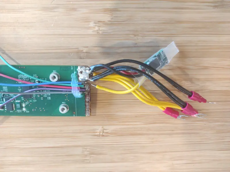 Yep, looks ugly, hot glue for strain relief of signal cables, small green pcb - dc-dc converter for 5V.
Overall, setup looks like this: 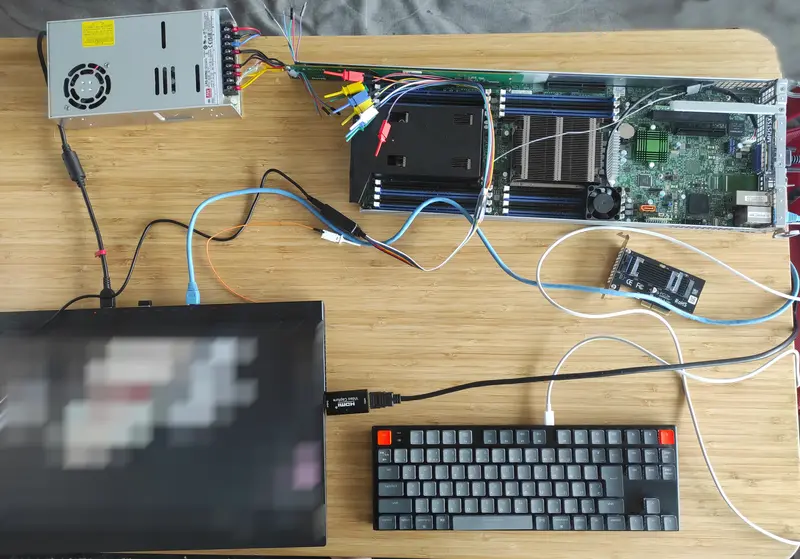
I started by hooking up logic analyzer to motherboard (A) side of connector, opening pulseview and turning PSU off/on we see: 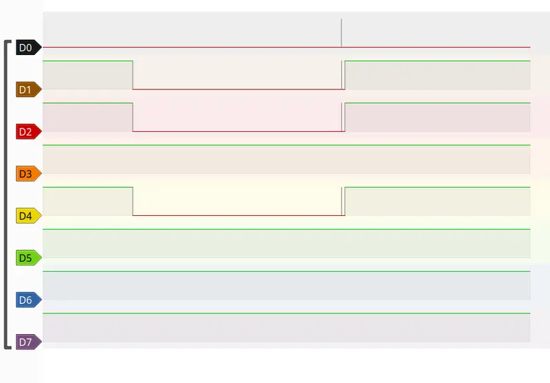
| Channel | Connector Pin | Voltage in S5/G2 state |
|---|---|---|
| CH0 | A27 | 0V |
| CH1 | A29 | 3.1V |
| CH2 | A28 | 3.1V |
| CH3 | A30 | 4.82V |
| CH4 | A25 | 2.8V |
What was weird is CH3 not turning off, but this could be due to poor contact.
Then I hooked up logic analyzer to case (B) side of connector, again, opening pulseview and turning PSU off/on we see...
Wait, it turned on?
Ok, it seems that logic analyzer weekly pulls pin up or down and fans start spinning, weird. Then I remembered - ATX PSU usually have two pins in thier connection PS_ON and PWR_OK.
- PS_ON is controlled by motherboard and pulled low to basically tell PSU to start providing 12V. Source
- PWR_OK is controlled by PSU and tells motherboard that PSU voltage is up to spec. Source
| Channel | Connector pin | Voltage in S5/G2 state |
|---|---|---|
| CH0 | B28 | 0V |
| CH1 | B32 | 0V |
| CH2 | B30 | 3.3V |
| CH3 | B31 | 3.2V |
| CH4 | B27 | 0V |
Observations:
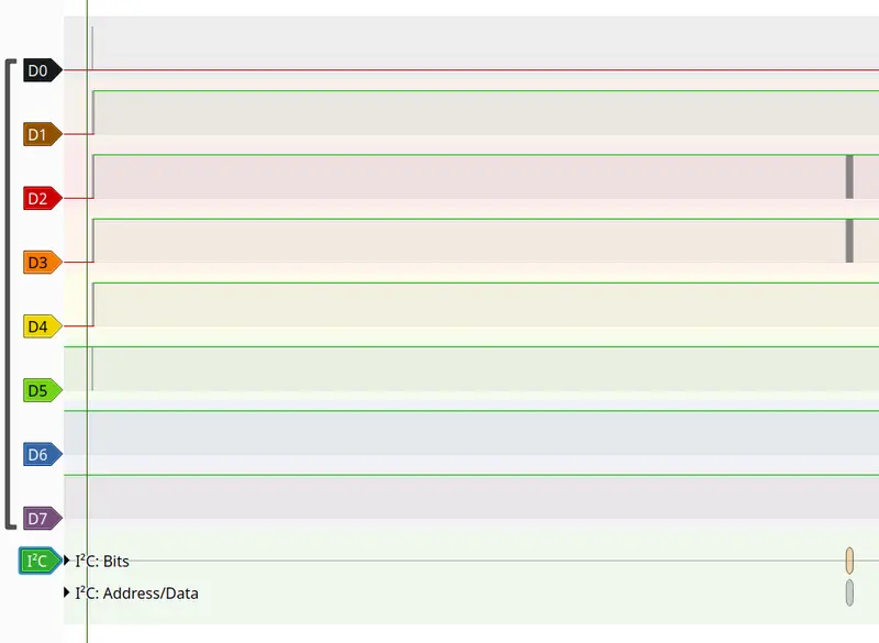
- D2 and D3 seems to push around some kind of data
- This means either D0, D1 or D4 is PWR_OK signal.
Let's figure out what is PWR_OK, by simply disconnecting logic analyzer from pins on at a time. And on first try - CH0, it turns off. Weird, PWR_OK as to spec should be held high. Taking another wire and connecting pin B28 to 5V through resistor turns system on. Ok, it seems that there is some discrepancy between logic analyzer and spec, but if it works, it works.
Now, let's figure out, what is happening on CH2 and CH3. 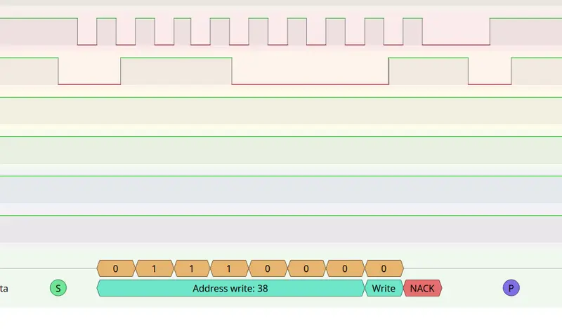
Zooming in and looking at it - looks preety much like I2C(SMBus) pair, enabling I2C decoder on the pins we see that it tries to access address 38 and getting NACK (Not acknoledged). So this is the way how motherboard usually communicates with PSU/backplane.
Now, going back to PWR_OK, CH0(B28 pin):
With CH0 pulled up to 5V though resistor, we get to boot. Checking IPMI Web UI we can see:
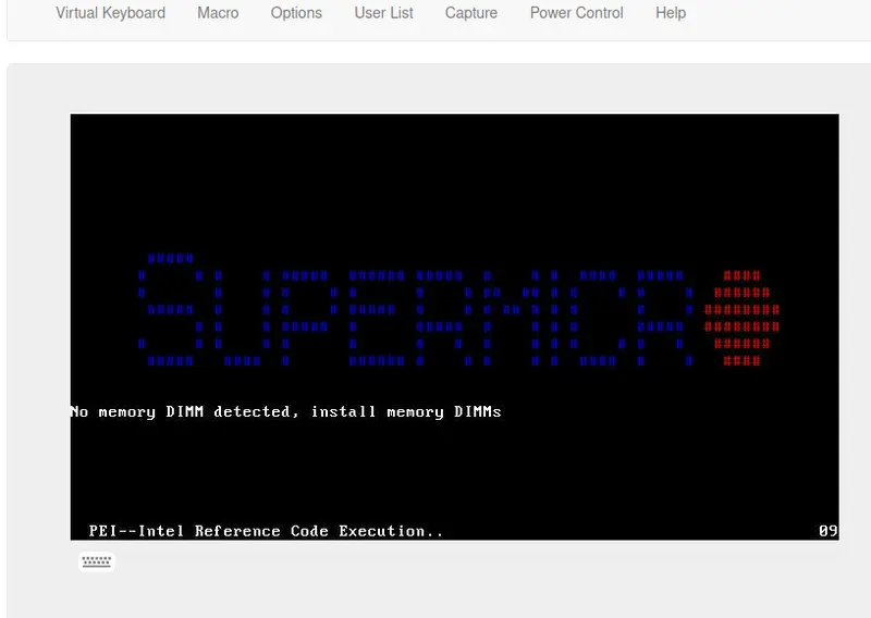
In next part, I am planning to go over designing and reciveing PCB, soldering all together, receiving ordered RAM and getting full OS boot.
Thanks for reading, When next part is available, link: Running DeepSeek-R1 on refubrished blade server: 03 Power+. (Intelligent Platform Management Interface) ↩
